Mon, August 17, 2026

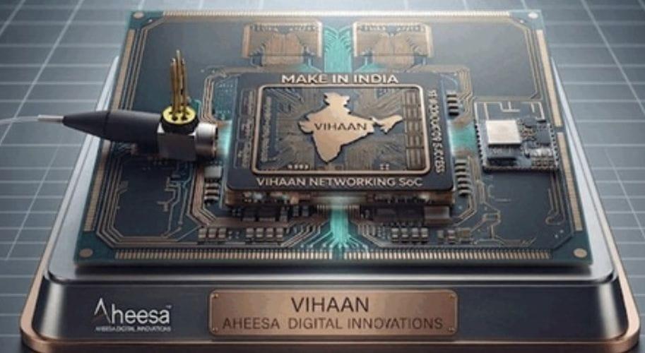
Photo: IANS
India’s semiconductor design ecosystem is showing signs of growing maturity, with domestic startups moving beyond chip development towards silicon validation and commercial production, aided by the government’s Design Linked Incentive (DLI) Scheme.
Chennai-based fabless semiconductor startup Aheesa Digital Innovations has achieved first-pass silicon success for its VIHAAN networking system-on-chip (SoC), designed for fibre broadband applications, the Ministry of Electronics and Information Technology (MeitY) said.
The chip was taped out on Republic Day and achieved first-pass silicon success on Independence Day this year. Aheesa is now preparing to move the VIHAAN chip towards production tape-out, which is targeted for 2027.
The development is significant because first-pass silicon success indicates that a chip has successfully moved from its design stage to functioning physical silicon without requiring a redesign. For a young semiconductor company, reaching this stage can substantially reduce development risks and bring a product closer to commercial deployment.
Aheesa is developing semiconductor solutions for broadband networking and security as India expands its digital infrastructure through optical fibre, 5G and broadband-based services.
The government's DLI Scheme is aimed at encouraging domestic chip design capabilities and supporting Indian startups working on semiconductor products for both commercial and strategic applications. These include satellite communications, drones, surveillance systems, defence and aerospace equipment, automobiles, IoT devices, artificial intelligence, telecom equipment and smart meters.
According to the government, semiconductor chip design can account for up to 50 per cent of the overall value addition across the semiconductor value chain. Chip design can also represent around 15-35 per cent of the bill of materials cost of electronic products, highlighting the economic importance of developing domestic design capabilities.
Aheesa has also attracted investment to accelerate product development and expand its operations. The company raised around Rs 40 crore earlier this year from the Tamil Nadu Emerging Sector Seed Fund and other private investors.
The broader DLI programme is also showing increased activity. Companies supported under the scheme have collectively completed more than 30 chip-design tape-outs across different foundries and have raised more than $100 million in venture capital funding, according to the ministry.
The government has also expanded access to semiconductor design infrastructure. Chip-design tools have been made available to 455 organisations, including 350 academic institutions and 105 startups. Under the Chips to Startup programme, 71 academic institutions have together taped out 245 chip designs.
Other recent semiconductor developments highlighted by the government include Vervesemi Microelectronics' motor controller chip, Netrasemi's 12 nm Vision SoC and OptoML's 12 nm compute-in-memory SoC.
The government has also approved the Semicon 2.0 programme with an outlay of Rs 1,27,500 crore. The initiative is intended to develop a globally competitive semiconductor ecosystem covering chip design, manufacturing, advanced packaging, equipment, materials, research and development and skilled manpower.
The progress of companies such as Aheesa suggests that India's semiconductor ambitions are increasingly extending beyond attracting manufacturing facilities to building indigenous intellectual property and chip-design capabilities. The transition of products such as VIHAAN from successful silicon validation to commercial production will be an important test of how effectively India's emerging chip-design ecosystem can convert government-backed innovation into globally competitive products.



© Copyright
Reporter Post.All Rights Reserved |
Powered by: Aptilogic Software |
 |
Page rendered in 0.074 seconds.
|
Page rendered in 0.074 seconds.