![]()
Mon, July 13, 2026
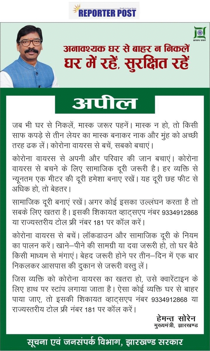
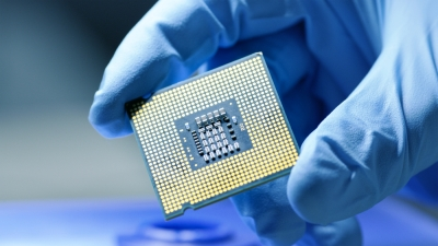
New Delhi — In a significant step towards advancing India’s semiconductor ecosystem, Union Minister for Electronics and Information Technology, Ashwini Vaishnaw, has approved the establishment of the ‘NaMo Semiconductor Laboratory’ at IIT Bhubaneswar, the Ministry of Electronics and IT (MeitY) announced on Sunday.
The project, estimated at Rs 4.95 crore, will be funded under the MPLAD Scheme, and is aimed at empowering India’s youth with industry-ready semiconductor skills while expanding the country’s growing talent pool in chip design.
According to MeitY, the new laboratory “will help position IIT Bhubaneswar as a leading centre for semiconductor research, training, and innovation,” adding that it will play a pivotal role in developing skilled professionals for upcoming chip manufacturing and packaging units across the nation.
The NaMo Semiconductor Lab is expected to serve as a catalyst for the ‘Make in India’ and ‘Design in India’ initiatives by supporting indigenous research and innovation in semiconductor design and fabrication.
Currently, India accounts for 20 per cent of the world’s chip design talent, with students from 295 universities leveraging advanced Electronic Design Automation (EDA) tools made available through industry partnerships. So far, 28 student-designed chips from 20 institutes have been successfully fabricated at SCL Mohali.
IIT Bhubaneswar was selected for the project owing to its expanding role in semiconductor research and its robust technical infrastructure. Odisha has also recently received approval for two semiconductor projects under the India Semiconductor Mission (ISM) — one focusing on Silicon Carbide (SiC)-based compound semiconductors and another on advanced 3D glass packaging.
The institute already hosts the Silicon Carbide Research and Innovation Centre (SiCRIC), and the upcoming lab will further strengthen its cleanroom and R&D capabilities.
Out of the total project cost, Rs 4.6 crore will be allocated for essential equipment and Rs 35 lakh for software necessary for semiconductor design, training, and fabrication.
With inputs from IANS


| 14-09-2018 | ||||||
| Sl No. | Parameters | Actual Data(µg/m3) | Standard Limit(µg/m3) |
|---|---|---|---|
| 1 | PM 10 | 64 | 100 |
| 2 | PM 2.5 | 33 | 60 |
| 3 | SO2 | 55.3 | 80 |
| 4 | NO2 | 58.2 | 80 |
| 14-09-2018 | ||||||
| Station | Temperature(degree centigrade) | Rainfall(mm) | Relative humidity(%) | |||
|---|---|---|---|---|---|---|
| Max | Min | Past 24 hrs. | Since 1st March, 2018 | Max | Min | |
| Ranchi | 31.0 | 22.5 | 000.0 | 1010.1 | 95 | 66 |
| Jamshedpur | 34.1 | 26.2 | 000.0 | 1252.8 | 87 | 58 |
| Bokaro | 33.5 | 24.6 | 015.2 | 824.0 | 92 | 79 |
| Daltonganj | 32.6 | 24.9 | 004.2 | 960.9 | 95 | 67 |
© Copyright
Reporter Post.All Rights Reserved |
Powered by: Aptilogic Software |
 |
Page rendered in 0.1003 seconds.
|
Page rendered in 0.1003 seconds.